In the next seven years, 2D semiconductor materials will usher in a critical stage from laboratory to industrialization, but epitaxial chip size will become the core development bottleneck. At present, 2D materials such as MoS₂ and WS₂ have achieved uniform growth on 4-inch wafers, but when moving towards 8-inch and even 12-inch wafers, they face challenges such as limited size of single crystal domains, increased defect density, and interfacial stress control. To break through this bottleneck, we need to rely on two major directions: one is to develop new selective epitaxy technologies (such as step-guided epitaxy) to induce the growth of single crystals in large domain regions through substrate lattice orientation; The second is to optimize the gaseous precursor CVD process to achieve uniform control of wafer-level thickness and electrical performance.
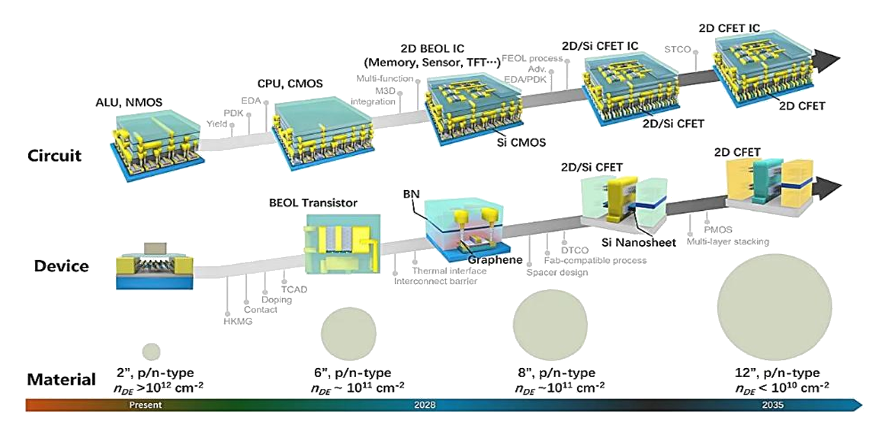
On the other hand, the atomic-level thickness of 2D materials and their excellent electrostatic control make them ideal for Monolithic 3D ICs (Monolithic 3D Integration). By stacking multi-layer 2D semiconductor channels and vertical interconnects (such as Buried Gate Array), the wiring congestion problem of traditional silicon-based FinFETs can be broken through and the 3D heterogeneous integration of logic and memory cells can be realized. For example, interlayer ultra-thin dielectric (h-BN below 1nm) based on 2D semiconductors can significantly reduce parasitic capacitance and improve the energy efficiency ratio of 3D chips. If combined with the low-temperature process (<400°C), it can also realize the direct integration of the back-end process (BEOL), providing a hardware foundation for emerging architectures such as storage and computing integration and neuromorphic computing.
In the future, the technology competition will focus on: 1) the autonomy of large-size monocrystalline two-dimensional material epitaxial equipment; 2) Heterobonding technology of 2D materials for 3D ICs; 3) Compatible design with silicon-based processes. If these bottlenecks are overcome, 2D semiconductors are expected to give birth to a new generation of ultra-compact, energy-efficient 3D integrated chips by 2030, reshaping the evolution path of Moore's Law.
With the maturity of two-dimensional material preparation technology, its market application is rapidly expanding from the field of scientific research to industrialization, and through the integration of existing industrial technology, it will provide new momentum for the transformation and upgrading of traditional industries. Future market growth will focus on three major directions:
1. Scientific research and industrial material demand:
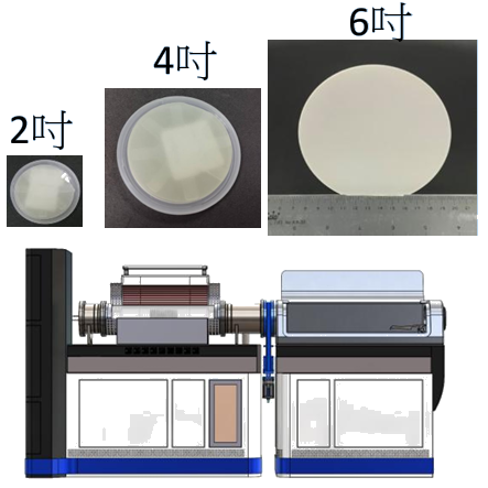
The high-quality, large-scale preparation of 2D materials will be the core driving force. The growing demand for diverse transition metal dichalcogenides (TMDs, e.g., MoS₂, WS₂) from research institutions and the semiconductor industry, especially on large wafer sizes (8 inches and above), will directly drive the market expansion of material preparation equipment (e.g., CVD systems). In addition, the application of two-dimensional materials in flexible electronics, photodetectors and other fields will also drive the commercial demand for high-purity and low-defect materials.
2. Biological and medical sensing market:
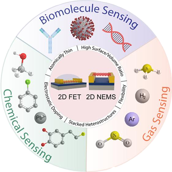
With their high sensitivity, biocompatibility and tunable surface properties, 2D materials have great potential in the field of medical sensors. For example, graphene or MoS₂-based PH sensors enable high-precision body fluid detection, while the application of functionalized 2D materials in DNA sequencing and biomarkers is expected to drive the upgrade of portable diagnostic devices. With the expansion of the precision medicine and wearable device market, 2D material sensors will become an emerging growth point.
3. Combination with third-generation semiconductors:
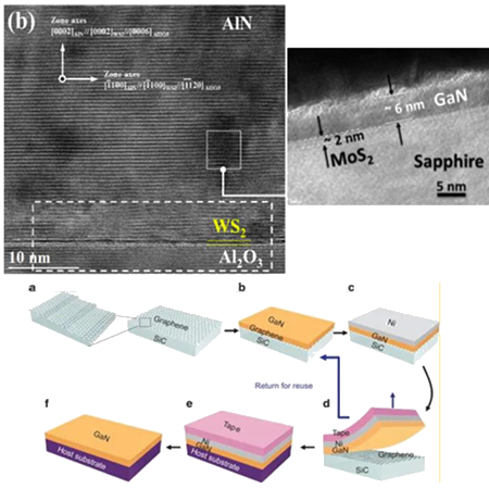
The heterogeneous integration of 2D materials with third-generation semiconductors such as GaN and SiC can optimize the performance of power and RF devices. For example, two-dimensional materials can be used as interface buffer layers to reduce the lattice mismatch problem of GaN-on-Si devices and improve device reliability. In SiC-based power electronics, two-dimensional insulating media (e.g., h-BN) can enhance heat dissipation efficiency. This convergence of technologies will provide more efficient solutions for high-end applications such as 5G communications and electric vehicles.
In summary, the development of the 2D materials market will rely on cross-domain technology integration, from scientific research equipment to medical sensing, and then to the third generation of semiconductor applications, gradually building a complete industrial chain and promoting global industrial upgrading.

Phone: (+86) 21 - 5899 6106 (+86) 21 - 5875 7196
Fax: (+86) 21 - 5899 6108
Postal Code: 200122
Address: Jiangsu Building 14F-C1,
#526 Laoshan Road, Pudong, Shanghai
