Size miniaturization alone is no longer a continuation of Moore's Law. The narrower the transistor channel, the more likely it is to affect the carrier transmission characteristics, because surface defects will dominate the transmission characteristics.
In the future, the development direction of sub-2nm node technology will focus on three core challenges: collaborative optimization of power consumption, performance, and integration.
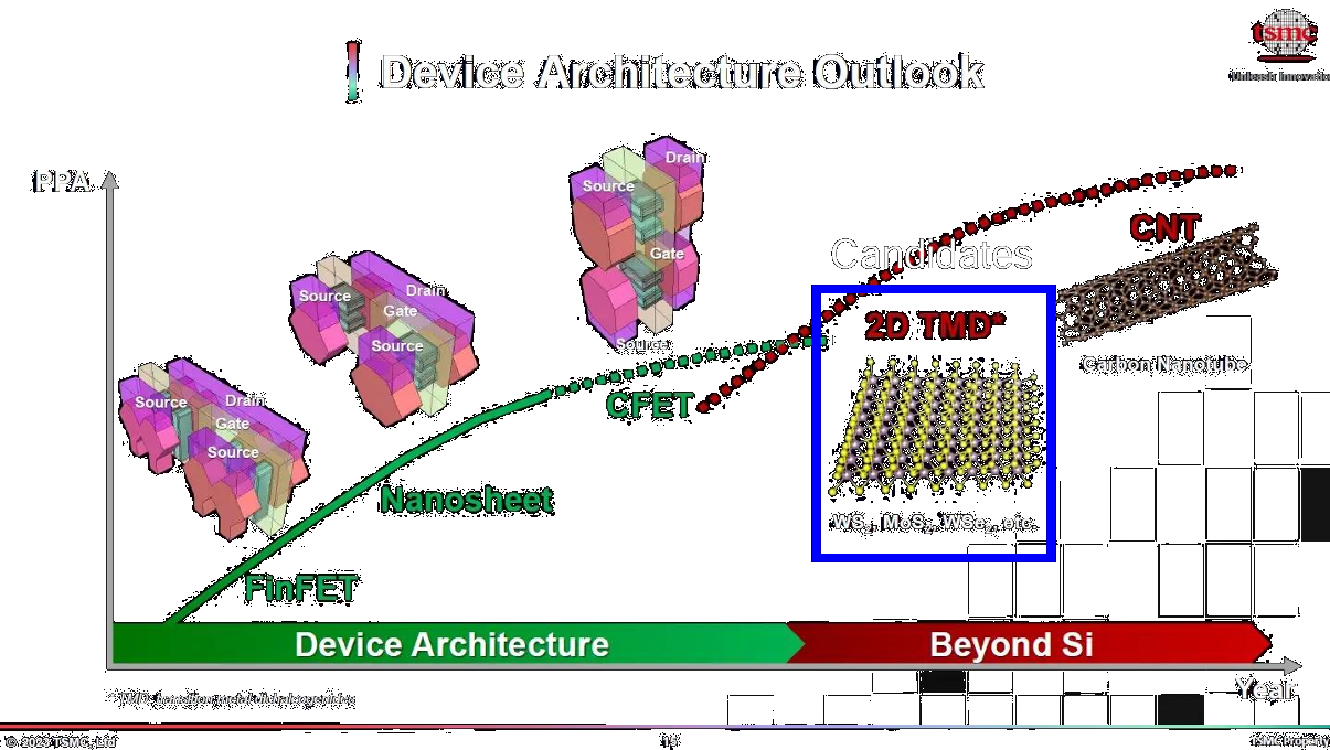
First of all, transistor architecture innovation is key. As FinFETs approach their physical limits, gate-around (GAA) nanosheet transistors will become mainstream, while more advanced CFETs (complementary field-effect transistors) and atomic-scale thin 2D materials such as MoS₂ may push the boundaries of the sub-1nm node to achieve higher density and efficiency through vertical stacking.
Secondly, breakthroughs in new materials and processes are crucial. High-NA EUV lithography (0.55 NA) will make the support more finely patterned, but it needs to solve the mask defect and cost problems; In terms of metal interconnects, cobalt and ruthenium replace copper to reduce resistance, while self-assembled molecular layers (SAMs) and selective atomic deposition (ALE) may enable atomic-level precision fabrication.
Finally, heterogeneous integration and 3D packaging will continue Moore's Law. Chiplet technology integrates different process nodes through advanced packaging (such as hybrid bonding), combines optical interconnection and near-memory computing, and compensates for the diminishing marginal benefit of scaling a single process with system-level innovation.
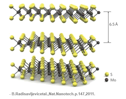
| Atomic thickness | ➥ | The gate pole of the device is easy to operate and the size is miniaturized |
| Atomic bonding within layers | ➥ | Covalent bonds tough |
| Between layers | ➥ | Van-der Waals force |
| Free of dangling bonds | ➥ | Component channel interface defects can be reduced |
| High carrier mobility | ➥ | High switching current, better electrical performance and more power saving |
At the nanoscale, two-dimensional semiconductors (such as MoS₂, WSe₂, etc.) exhibit excellent electrical properties far beyond traditional silicon-based materials, with carrier mobility up to nearly 100 times that of silicon semiconductors, and at the same time have perfect electrostatic control and extremely low leakage current characteristics brought by atomic-level thickness. These characteristics make 2D semiconductors a key material to break through the sub-1nm technology node, which can not only complement the CFETs architecture, but also enable multifunctional device innovation through heterogeneous integration.
With large-scale growth and breakthroughs in interface engineering technology, 2D semiconductors are expected to set off a new round of material revolution in the post-Moore era, providing disruptive solutions for high-performance computing, low-power chips and new memory devices.

Phone: (+86) 21 - 5899 6106 (+86) 21 - 5875 7196
Fax: (+86) 21 - 5899 6108
Postal Code: 200122
Address: Jiangsu Building 14F-C1,
#526 Laoshan Road, Pudong, Shanghai
