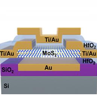
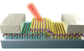
Two-dimensional (2D) materials have shown revolutionary potential in cutting-edge fields such as artificial intelligence chips, image sensing, and flexible electronics. In terms of artificial intelligence chips, semiconductor 2D materials such as MoS₂ can realize ultra-low-power neuromorphic computing devices with atomic-level thickness and high carrier mobility, and their natural bipolar characteristics are particularly suitable for simulating synaptic behavior, providing a new solution for the integrated storage and computing architecture. Graphene's high conductivity and thermal stability can optimize chip interconnects and improve the energy efficiency of AI accelerators.
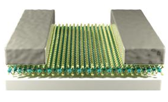
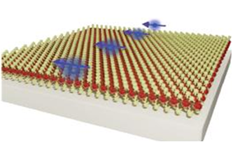
In the field of image sensing, the wide spectral response characteristics of 2D materials (such as black phosphorus covering the mid-infrared to visible light band) open up a new path for the design of high-sensitivity, ultra-thin image sensors. By stacking 2D materials with different bandgaps (such as MoS₂/WSe₂ heterojunctions), multispectral detection pixels can be constructed, which greatly improves the environment perception ability of machine vision.
For flexible electronics, the mechanical flexibility and transparency of 2D materials (e.g., graphene light transmittance >97%) make them the preferred material for wearables and e-skin. For example, flexible transistors based on WS₂ can withstand thousands of bends, while graphene strain sensors can monitor human movement in real time. In the future, the integration of 2D materials with flexible substrates, such as polyimides, will drive the rapid development of foldable displays and biomedical sensing.
The core challenge in these directions is to achieve uniform wafer-level 2D material growth and compatibility with existing processes, but once it does, it will reshape the technology landscape for the next generation of smart hardware.
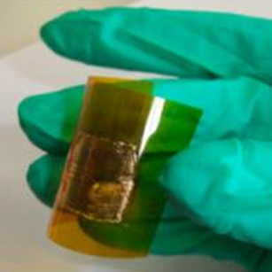
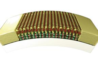
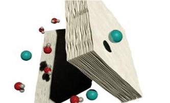
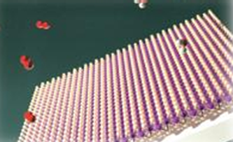
Two-dimensional (2D) materials are revolutionizing many fields due to their atomic-level thickness and unique physicochemical properties.
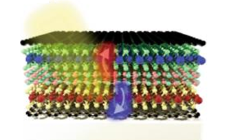
In the semiconductor industry, transition metal diccogenides such as MoS₂ are expected to break through the 1nm process node and become channel materials for next-generation transistors. In the energy field, graphene supercapacitors can be charged in seconds; In the biomedical field, flexible 2D material sensors can monitor physiological signals in real time; In the field of optoelectronics, the broad-spectrum response characteristics of black phosphorus help the development of ultra-thin infrared imaging chips; In the aerospace sector, 2D composite coatings can significantly improve the corrosion and radiation resistance of materials.
These breakthrough applications highlight the enormous potential of 2D materials as revolutionary platform materials.

Phone: (+86) 21 - 5899 6106 (+86) 21 - 5875 7196
Fax: (+86) 21 - 5899 6108
Postal Code: 200122
Address: Jiangsu Building 14F-C1,
#526 Laoshan Road, Pudong, Shanghai
