Our innovative all-gaseous precursor CVD (Chemical Vapor Deposition) equipment provides a new technical path for the preparation of 2D materials. Different from the traditional preparation method that relies on solid powder precursors, the equipment adopts a full gas phase reaction system, and realizes the essential improvement of the two-dimensional material growth process through the precise ratio and control of well-designed metal-organic compounds and chalcogenide precursors.
Compared with the limitations of the traditional powder method, the all-gaseous system shows significant advantages: the precursor can be mixed and transported more uniformly in the gas phase, which greatly improves the uniformity and repeatability of material growth; By precisely controlling the flow rate and proportion of the reaction gas, the growth kinetics of the material can be controlled more flexibly. The prepared two-dimensional materials have better crystallization quality and lower defect density.
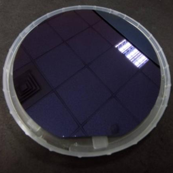
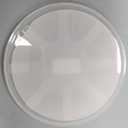
The equipment supports the large-scale preparation of wafer-level 2D semiconductor materials, and has reached the advanced level in terms of film uniformity, crystal quality and electrical properties. This innovative design not only overcomes the inherent limitations of traditional preparation methods, but also provides reliable mass production equipment support for the application of 2D materials in the semiconductor industry.
| CVD/Precursor Type | Wafer Size | Process Maneuverability |
Uniformity | Quality | Mass Production Feasibility |
| Hotwall/Solid Powders | Fragment~2inches | Lower | Lower | High | Not Good |
| Hotwall/Fully Gaseous | 2~6inches or more | High | High | High | Excellent |
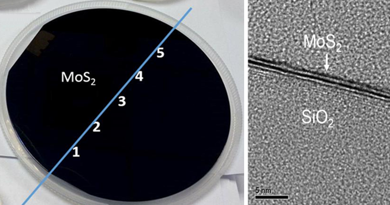
Transition metal dichalcogenides (TMDCs) such as MoS₂, WS₂, and WSe₂ can be uniformly grown on 4-inch silicon wafers and sapphire substrates via optimized chemical vapor deposition (CVD) processes. For silicon wafers, a thermally oxidized SiO₂ surface is typically employed to facilitate nucleation and lateral growth, while single-crystal sapphire substrates enable epitaxial growth of TMDC monolayers with preferred orientations due to lattice matching effects.
Key advancements in large-area growth involve precise control of precursor stoichiometry (e.g., MoO₃ and S for MoS₂), gas flow dynamics, and temperature gradients to ensure thickness uniformity and full coverage. Post-growth characterization reveals high crystal quality, with photoluminescence spectra showing strong excitonic peaks and Raman mappings confirming monolayer homogeneity across the wafer. These wafer-scale processes achieve electronic-grade TMDCs with field-effect mobility exceeding 100 cm²/V·s, making them viable for integration with conventional semiconductor fabrication lines. The choice between silicon and sapphire substrates depends on target applications—silicon for CMOS-compatible electronics versus sapphire for optoelectronic devices requiring transparency.

Phone: (+86) 21 - 5899 6106 (+86) 21 - 5875 7196
Fax: (+86) 21 - 5899 6108
Postal Code: 200122
Address: Jiangsu Building 14F-C1,
#526 Laoshan Road, Pudong, Shanghai
